
Trusted measurement data for semiconductor manufacturing
Humidity, dew point, temperature, pressure, and wet chemical concentration measurements that autonomous fabs, AI, and digital twins can trust. From cleanroom to machines to gas lines to wet bench.
semiconductor fabs are our customers
member
Next-gen semiconductor fabs operate autonomously.
The enabler is reliable measurement data.
In industry roadmaps, AI, digital twins, and automated control act on every sensor reading, often without a person checking it first.
Vaisala's humidity, dew point, temperature, pressure, and wet chemistry concentration measurements give your fab data it can act on, from the cleanroom to the gas line to the wet bench.
Stable
Measurements that stay true between calibrations. Our HUMICAP® and DRYCAP® sensors are built for long-term stability and low drift, so your models are not chasing sensor error.
Verifiable
Traceable calibration, and smart probes. You know when to trust a reading and when to act.
Connected
Digital probes and the Indigo platform plug into tools, facility monitoring systems and data platforms with various supported protocols. Data arrives clean and ready to use.
Low lifetime cost
Long calibration intervals, swappable probes, and fewer site visits equal lower lifetime costs.
Guarantee success with trusted measurements
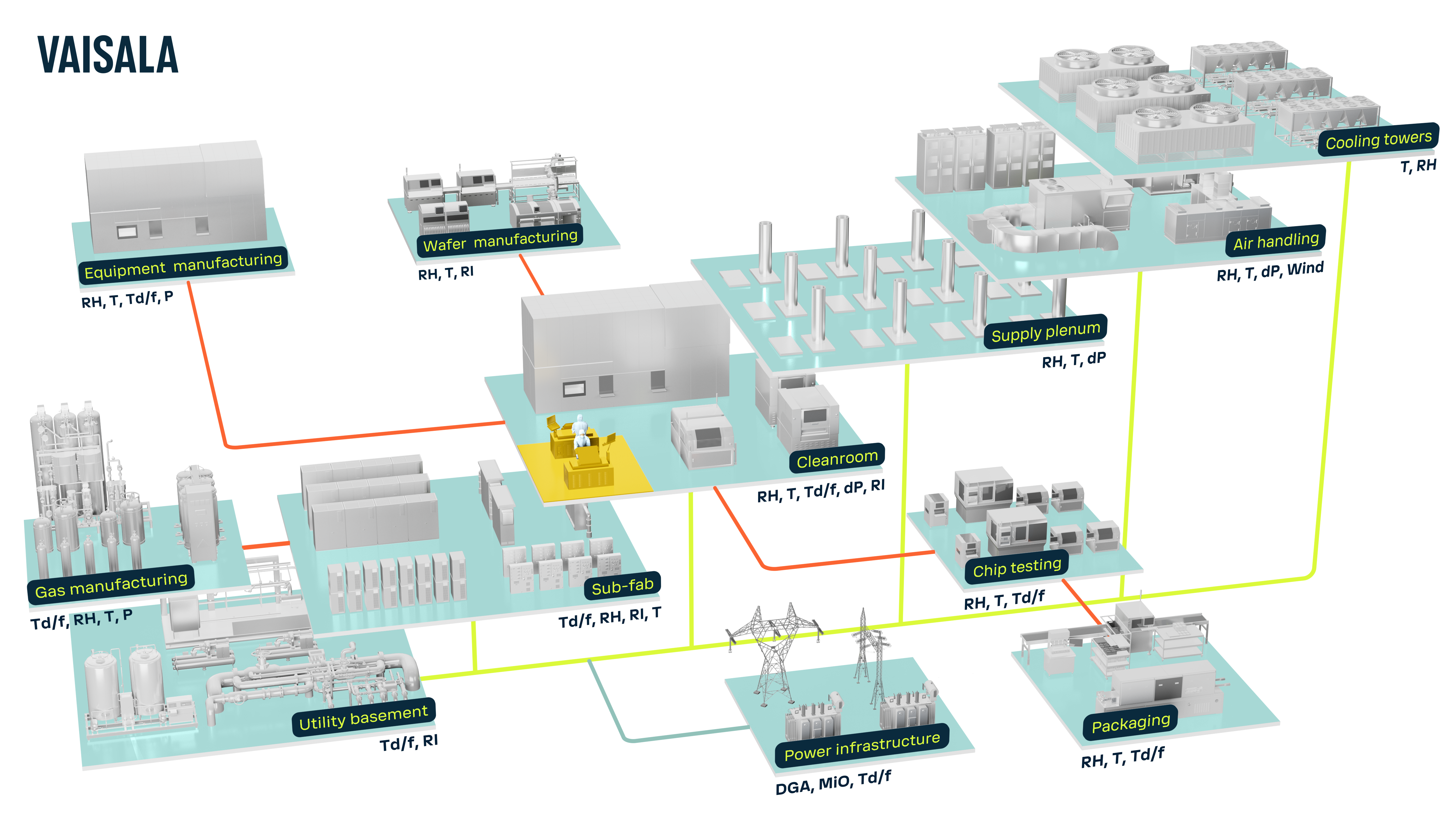
One trusted measurement data source, from wet to dry and back
From semiconductor wafer manufacturing, and microelectronics fabrication to packaging semiconductors, equip your critical processing steps with trusted and reliable measurements for stable quality, high yield, predictability, and cost-efficiency.
Our offering covers instruments measuring humidity, dew point, temperature, pressure, and wet chemistries’ concentrations. Each product produces precise data on the manufacturing environment, and provides superior accuracy, long-term stability, and rapid response time for process optimization, increased yield, safety and best-performing chips.
For these reasons, Vaisala is the preferred measurement partner for semiconductor manufacturers and MEMS foundries, semiconductor equipment manufacturers and OEMs, fab operators, and material suppliers.
From the front-end to back-end and all the way to the customer, we've got you.
For everyone who shapes the fab
Fab operators and facility teamsStable data for yield, uptime and autonomous operation | Equipment makers and subsystem suppliersSensors that integrate easily into your tool and carry your quality to every fab you ship to | |
Designers, contractors and integratorsSpecification support, ISO 14644, and URS/FAT/SAT documentation | Gas and material suppliersDew point measurements, trace moisture data that prove purity from the plant to the point of use |
Explore solutions for
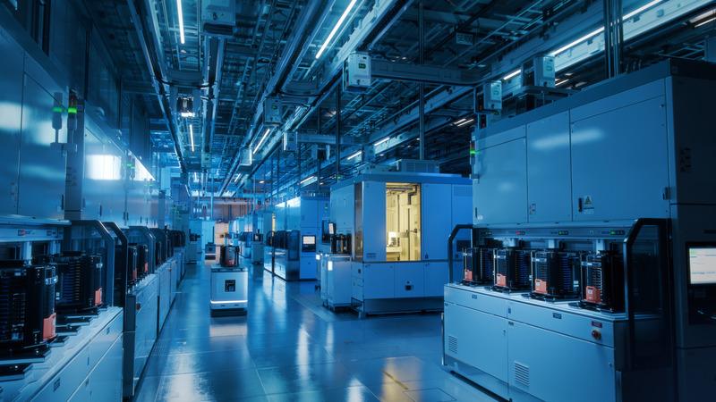
Cleanroom and HVAC
Humidity, temperature and differential pressure for ISO 14644 cleanrooms and photolithography areas with humidity tolerances as tight as ±0.8 %

Inside the tool
Compact humidity, temperature and dew point sensors designed into semiconductor equipment, from photolithography to steppers to probers to wafer cleaning
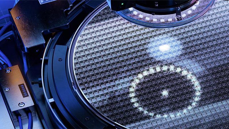
Wet chemistry
Semiconductor wafer plants consume tons of chemicals throughout the fab process. Ensure each chemical's reliability and avoid specification deviations that can result in expensive equipment contamination and wafer scrap.
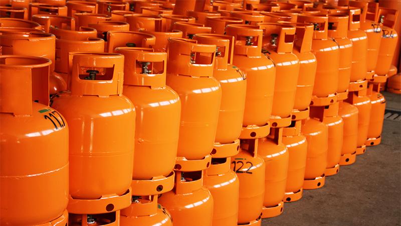
Ultra-pure gases
Protect expensive process gases from being contaminated by humidity. Gas quality significantly affects chip quality, as even trace impurities can lead to defects or failures. Moisture can react with certain materials or introduce defects during processes like oxidation. A rapidly reacting probe will detect any moisture quickly and alert when reaching the set limit.
Why Vaisala
Designed for semiconductor manufacturing
Vaisala's comprehensive offering with just the right parameters provides stable measurements in semiconductor manufacturing.
Measurement accuracy designed in the product
Select products surrounded by an ecosystem of support, with optimized cost of ownership and with minimum lifecycle costs.
Avoid risks - select reliable products from wet to dry
Vaisala's products cover the whole measurement range, and everything you need from wet to dry, including products for specific applications.
Tailored products - Engineer-to-Order
Did you know that our products can be customized for a specific application or installation position?
Nothing gives us more joy than to solve difficult measurement problems, together with you. Contact us! We are here to help.
We walk the walk
Vaisala produces sensor chips for Vaisala products, and for R&D use in our own in-house cleanroom. We know what it takes to produce world-class quality.
In addition, Vaisala is committed to supporting our products throughout their entire lifecycle, and our expert services and support are located near you, wherever you are.
Expert content and customer cases
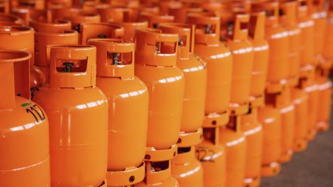
Dew point measurements best practices in semiconductor dry gases and wafer testing
Semiconductor ultra-pure gas can get contaminated down the line, and even trace moisture can ruin a chip. Learn how to keep your ultra-pure gases truly dry in this 30-minute, free webinar.

Why humidity measurements matter in semiconductor manufacturing
In semiconductor manufacturing nothing matters more than accuracy. One of the most critical parameters to measure is humidity, as maintaining exactly the right moisture levels is crucial for optimal equipment performance and end-product quality.


Comparação de tecnologias
Analise como a sonda de ponto de orvalho da Vaisala se compara ao CRDS (Espectrômetro de Decaimento de Cavidade)
e transmissores de espelho resfriado nos ambientes operacionais mais exigentes, como
Fabricação de baterias recarregáveis e de semicondutores.
| Sonda de ponto | de orvalho de VaisalaMedição Td do transmissor | de espelho resfriado CRDS | |
alcance* | -80 °C...+20 °C-100 | °C...-50 °C | -70 °C...+20 °C |
| Medição | in situ Sim | Não, requer amostragem e uma grande diferença | de pressão Não, requer amostragem |
| Precisão Td em Condições laboratoriais* | +/-2 °C | +/-0,2 °C | +/-0,2 °C |
| Faixa de pressão* | 1... 50 bar | 1... 5 bar | ~ apenas |
| 1 barra Dependência de atmosférico Condições | Não dependente | Dependente. Condições atmosféricas estáveis são necessárias. A amostragem pode gerar erros em ambiente não laboratorial. ambiente. | Dependente. O ponto de orvalho mínimo aumenta se a temperatura ambiente aumentar. A amostragem pode gerar erros em ambientes não laboratoriais. |
| Tempo de resposta* | Minutos | Dezenas de minutos | Horas |
| Sensibilidade | Alta | Baixa (não detecta mudanças rápidas, média da medição) | Baixa (não detecta mudanças rápidas, média da medição) Tamanho: |
| Pequeno e leve. Encaixa facilmente em vários locais | Médio porte, cerca de 10 kg | De grande e pesado a médio | |
| Operador para fornecer serviço regular | Não necessário | Não necessário | Necessário |
| Componentes que necessitam manutenção serviço | Não necessário | Não necessário, se em ambiente limpo | Necessário (ex.: Peltier) |
| calibração local/ Suporte disponível | Sim | Improvável | Improvável |
| Dependência de gases de fundo | Menor | Potencialmente forte | Potencialmente crucial |
* Valores típicos na fabricação de baterias e semicondutores
Semiconductor manufacturing related products
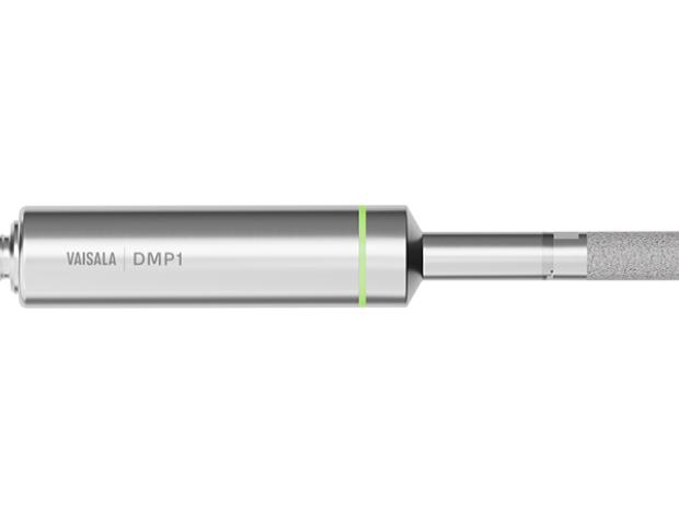
Dew Point Probe DMP1
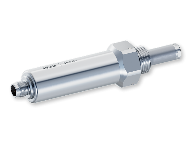
Dew Point Transmitter DMT153
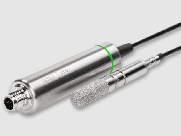
Dew Point and Temperature Probe DMP7
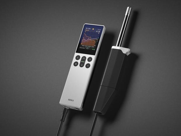
Indigo80 handheld measurement device
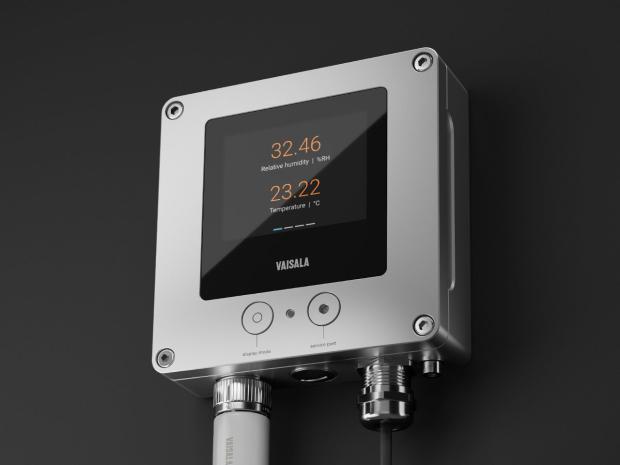
Indigo300 transmitter
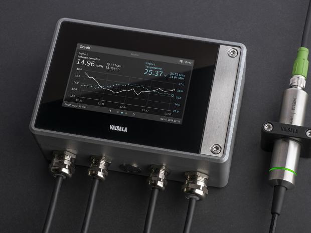
Indigo500 Series Transmitters
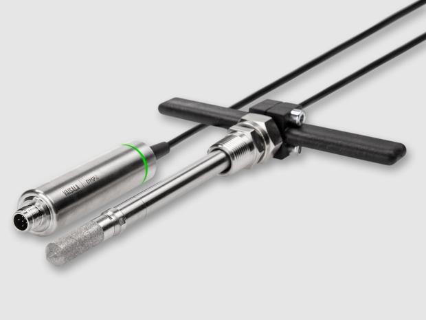
Dew Point and Temperature Probe DMP8
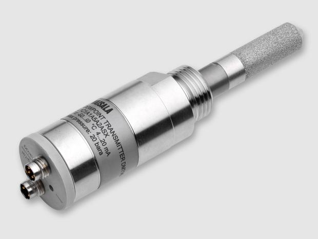
Miniature Dew Point Transmitters DMT143 & DMT143L (Long)
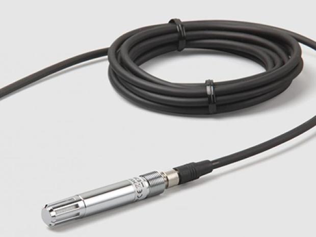
Humidity and Temperature Probe HMP110
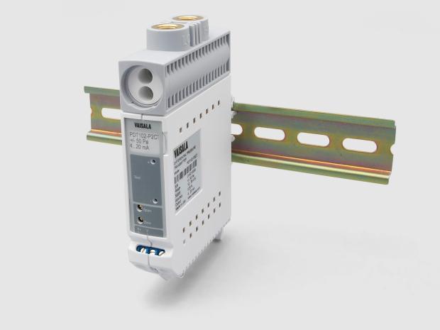
Differential Pressure Transmitter PDT102
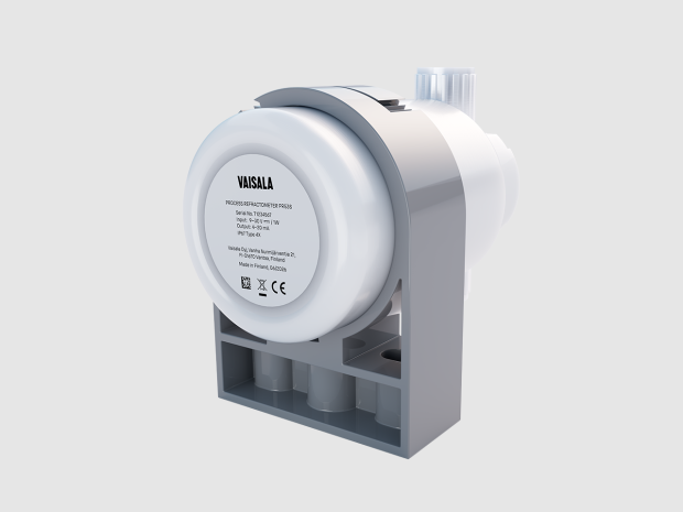
Vaisala Polaris™ PR53S Semicon Process Refractometer
Qual é o instrumento mais adequado para medir o ponto de orvalho?
Ready start building your fab on data you can trust?
Talk to our semiconductor experts about cleanroom, machine, gas and wet chemistry measurements for your project.
Semiconductor manufacturing other applications

Wafer cleaning with the help of durable products
Wafer cleaning is a critical process in semiconductor manufacturing for removing contaminants, particles, and residues from the surface of silicon wafers. This process ensures the reliability and functionality of integrated circuits (ICs) and other semiconductor devices.
Extra durability
Cleaning agents can include acids, various solvents, and water, and these residues might be present, thus requiring extra durability from measurement probes.
Vaisala offers corrosive resistant probes also without metal wetted parts, specially tailored for the wafer cleaning process, tolerating both high humidity and harsh chemicals.
It is important to ensure chip dryness after cleaning to prevent contamination and particle adhesion.
Temperature control for zero variations in the wafer patterns
Quality measurement probes in steppers offer stable temperature measurements and safeguard wafers from having variations in dimensions of the patterns induced by temperature fluctuations. Wrong dimensions on wafer patterns adversely affect the overall quality and performance of the semiconductor devices.
Humidity control for optics stability
The wafer stepper relies on precise optics to project and transfer patterns onto the wafer. Any variations in temperature or other environmental conditions can affect the stability and accuracy of these optics.
Barometric pressure control for accurate lithography, and process stability
Measuring barometric pressure is a must for optical precision and accuracy of the lithography process as barometric pressure directly influences the refractive index of air, which in turn affects the optics of the wafer stepper and the wavelength of lithography light.
Focus and depth control
Prevent defocused images by measuring and controlling barometric pressure with fast and accurate measurement instruments.
Wafer stepper in photolithography
Wafer stepper in photolithography is another critical processing step in the production of integrated circuits (ICs) and other semiconductor devices. In this step, a light pattern is projected onto a silicon wafer coated with photosensitive material (photoresist), thereby etching the desired pattern onto the wafer. As a result, some photolithography areas may have humidity tolerances as tight as ±1%.

Maintain chip prober machine ice-free with humidity control
The wafer probing machines identify defective wafers by testing chips. Tests are performed in cold temperatures, up to -40 Celsius ( -40 Fahrenheit) to ensure the chip works in extreme temperatures, for example, if later intended to be used in a vehicle.
The test environment must be kept dry, with the dew point temperature under -40 so that there is no ice deposition on the chip, which would later, when transferred to room temperature, turn to water and collect impurities on the chip.
Vaisala offers accurate dew point probes for the chip prober machines.


