World class circuit pattern positioning in photo lithography: the wafer stepper

Producing nano-scale circuit patterns enables faster and more complex operations in the ICs while consuming less power, which is crucial for future technologies. By utilizing accurate process monitoring and advanced technologies, it is possible to achieve circuit patterns as small as 3-5 nanometers (nm), or even 1-2 nm. However, even minor deviations in the photolithography process—such as misalignment, particle contamination, or variations in exposure and development—can lead to significant yield reductions that impact production efficiency and increase costs.
The process steps: the wafer stepper
Manufacturing ICs involves a long chain of process steps, as shown in Figure 1. Before the photolithography step, a photoresist coating is applied onto the wafer. This light-sensitive coating protects certain areas of the wafer that will be exposed to light during the lithography process. After the photolithography step, unwanted material is removed to create the desired structure during the developing and etching stages. Etching removes unwanted material, and doping adjusts electrical properties. These steps are repeated to build circuit layers. Finally, the wafer is inspected for defects and diced into individual chips.
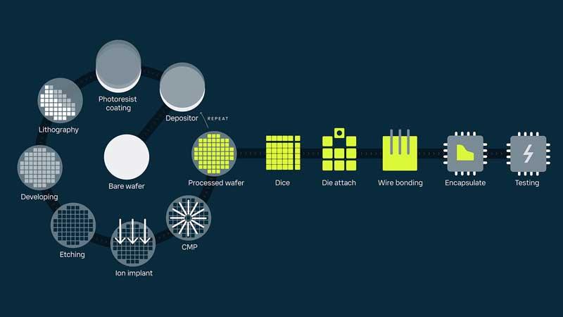
Figure 1: The process of making ICs
Exposure systems for wafer steppers in photolithography
Figure 2 illustrates an exposure system in which the wafer stepper is located. The exposure system operates in a clean room environment, where the Indigo520, along with HMP3/HMP7, monitors humidity, temperature, and pressure. This setup ensures a stable and controlled environment for the sensitive process of photolithography and the wafer stepper.
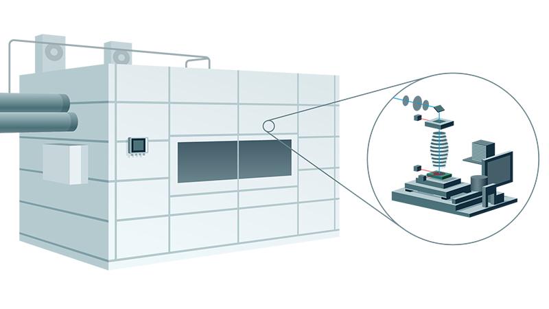
Figure 2: Exposure system for the wafer stepper
Wafer stepper
The wafer stepper, illustrated in Figure 3, is responsible for printing the circuit pattern on a wafer. Accurate positioning of the stepper is crucial and is achieved through precise measurements of absolute pressure, humidity, temperature, altitude, and laser frequency.
Pressure is the predominant source of error, contributing to more than half of the total inaccuracies. Monitoring and controlling these five parameters enable accurate wavelength correction, which is essential for precise circuit pattern positioning on the wafer.

Figure 3: Wafer stepper

Instrumentation
Vaisala’s Indigo520 transmitter, equipped with a barometric pressure measurement module and one or two Indigo-compatible humidity, dew point, and temperature measurement probes, offers a unique combination of key parameters in a single industrial device. It measures three parameters simultaneously: barometric pressure, humidity/dew point, and temperature.
The device incorporates Vaisala's proprietary HUMICAP®, DRYCAP®, and BAROCAP® technologies. Furthermore, the DMT143 or DMP7 is used to monitor the dew point level of the stepper.
Pressure measurement
| Indigo520 | PTB330 | Barometer | |
| Accuracy | ±0.15 hPa | ||
| Response time T63 | 2 s | ||
| Measurement range | 500–1100 hPa |
Humidity and dew point measurement
| HMP3/ HMP7 | DMP7 | DMT143 | |
| Accuracy | ±0.8 %RH | ±2 °C Tdf | ±2 °C Tdf |
| Response time T63 | 15 s | 5 s | 5 s [15 s] |
| Measurement range | 0–100 %RH, at max. +95 °C (203 °F) Td | −70 … +80 °C Tdf | −70 … +60 °C (−94 … +140 °F) Td |
For all applications and measurement solutions go to vaisala.com/semicon