Introduction
Vaisala K-PATENTS® Semicon Refractometers PR-33-S/-23-MS are designed for real-time concentration monitoring of wet chemicals used in the silicon wafer fabrication. The refractometer provides a continuous measurement signal (4-20 mA or Ethernet output), which offers many possibilities for real-time monitoring and process controlling. Due to the unique digital measurement principle there is no signal drift.
The main benefit of the real-time monitoring with the refractometer is the potential yield improvement in the form of increased wafer throughput. This is achieved through extended bath life and the optimization of chemical consumption. The exact chemical flow depends on bath chemistry and sequence, chemical concentration, cleaning time and temperature. The purpose is to process more wafers with an optimized chemical volume and to minimize equipment down times in the entire wafer handling process.
Certain wet chemicals require a separate disposal system. The waste streams are typically not amenable to internal recycling or reuse. Consequently, both economic and environmental savings in the waste chemical treatment can be achieved with the optimized use of chemicals.
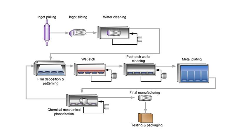
Application
Wafer Cleaning
Wafer Cleaning is performed by using various liquid chemicals to remove contaminants from the surface of a silicon wafer. The most commonly used method is the RCA clean process, where RCA-1 clean, also called SC-1 (Standard clean 1), is used for the removal of organic residues and particles. RCA-2 clean, or SC-2 (Standard clean 2), cleans metal contaminants from the wafer. Diluted HF and SPM remove Silicon oxides and heavy organics respectively. The PR-33-S/-23-MS provides a method for monitoring the point of use (POU) blending and delivery of the chemicals.
Wet Etch
Wet etching is used to chemically remove layers (metal, silicon, photoresist) from the surface of a wafer during manufacturing. Etchants, which erode the substrate equally in all directions, are called isotropic. Modern processes prefer anisotropic etches because they produce sharp, well-controlled features.
Several anisotropic wet etchants are available for silicon. For instance, potassium hydroxide (KOH) and Tetramethyl ammonium hydroxide (TMAH) are commonly used for this purpose.
The etch rate of silicon in a KOH bath depends on the bath temperature and the KOH concentration. Silicon etch rate is a function of the KOH concentration and bath temperature. As etching progresses, some KOH (namely OH- ions) is consumed in the process. We provide an indication of KOH concentration and helps to determine the correct etch end-point. This way the bath life can be increased, and wafer scrap and chemical waste can be minimized.
The refractive index gives an indication of the total of dissolved solids. The etching of silicon using a KOH water mix forms a tertiary solution with the dissolved silicate. The influence of the Silicate needs to be compensated from the KOH concentration reading. We provide a method (patent pending) for compensating this in the refractometer output reading. The compensation factor can be implemented in the control system. The same phenomenon is seen in the etching of Silicon nitride with hot phosphoric acid.
Post-Etch Wafer Cleaning
The purpose of the post-etch wafer cleaning is to remove residues from the wafer. Post-etch cleaning is typically accomplished by Amine (e.g. Hydroxyl amine), Fluoride or Quaternary (e.g. NMP) based chemicals.
The refractometer measures the concentration of the post-etch cleaners, for example, polymer remover such as EKC. This provides a real-time indication of the bath life time, which assists in increasing the wafer throughput and achieving significant savings in the chemical consumption.
Chemical Mechanical Planarization
In order to make the wafer surface smooth after the metal deposition, a method called Chemical Mechanical Planarization (CMP) is applied. Excessive metal is removed by using abrasive CMP slurries, which typically contain silica or alumina particles and a moving polishing pad. Bulk dispensing and blending methods are needed because of the large quantities of slurry, which are required in high-volume manufacturing fabs.
Typically, CMP processes use hydrogen peroxide (H2O2) as an oxidizing agent in the slurries. Hydrogen peroxide requires on-site blending as it has a short pot life and is not stable for long enough to permit shipping. Tight control of the hydrogen peroxide when blending the mixture is important, since too much of it can result in wafer contamination.
The PR-23-MS provides a real-time method for the concentration monitoring of H2O2 in the POU blending of the CMP abrasive slurries.
Further Processing
After the wafer surface is polished, the wafer processing starts all over again with film deposition, patterning and etching. Layer after layer is created on the wafer. Between each step, the transistors are connected with copper or aluminum interconnects. The interconnects are separated from each other with insulators. One microchip can have up to ten layers of interconnects.
Instrumentation and installation
The Semicon Refractometer monitors the chemical concentrations in real-time and provides immediate feedback of chemicals reaching their out-ofspecifications limit. The refractometer can be used in the bulk chemical delivery systems in the sub-fab, in the point-of-use chemical blending and spiking applications in the cleanroom.
Refractive index has proven to be a reliable parameter to monitor chemical purity, quality and blending, and also for chemical identification during semiconductor manufacture.

Vaisala K-PATENTS® Semicon Refractometer PR-33-S
A small footprint, PVDF covered sensor for cleanroom environment and integrated process tools. Monitors the chemical concentrations in real-time and provides an Ethernet output signal and immediate feedback to the control system. Connected through a modified PTFE flow cell body to the process by a 1/4”-1” Nippon pillar or flare fitting.
Measurement range
Refractive Index (nD) 1.3200 – 1.5300, corresponding to 0-100 % by weight.